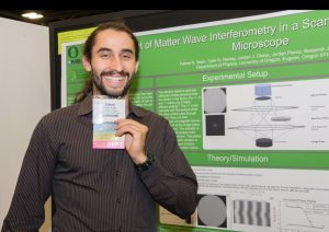
Fehmi Yasin was lead author and presenter on the poster “Development of STEM-Holography” for the Microscopy & Microanalysis (M&M) conference in Colombus, Ohio last week. M&M is one of the premier international conferences for discussing all types of microscopy-related research, and draws researchers and engineers from many different areas of science and industry. It also draws scientists like us interested in electron physics.
In this work, Fehmi and the other authors (Tyler Harvey, Jordan Chess, Jordan Pierce, and myself) discuss our use of a single nanofabricated diffraction grating to divide a beam of electrons inside an electron microscope, such that each electron in the beam moves along two separate paths at the same time (one of those interesting effects allowed by quantum physics). Fehmi and the other authors are developing ways to use this technique to image difficult-to-see structures at the nanoscale inside a transmission electron microscope (TEM).
In addition to getting a Student Meeting travel award to attend this meeting, upon presenting the poster Fehmi also won First Place poster prize for “Advances in Instrumentation”! Thank you to the Microscopy Society of America (MSA) for sponsoring both of these awards. Thank you also to Tyler, Jordan C, and Jordan P for all your help to Fehmi on this exciting project, and for all of your contributions and great feedback on the poster!
Fehmi Yasin won a Student Meeting Award to attend the 2016 Microscopy & Microanalysis meeting, for his paper titled “Development of STEM Holography”. His award is sponsored by the Microscopy Society of America (MSA) and the Microanalysis Society (MAS). The award includes complimentary student registration for the full M&M 2016 meeting and financial support to help defray expenses to attend the meeting. Great job, Fehmi!
It was announced this summer that I received a 2013 Early Career Award from the U.S. Department of Energy (DOE) for the proposal to develop “Electron Microscopy with Vortex Beams Carrying Orbital Angular Momentum”. I’m very honored and humbled to receive this award, as this was among only a handful of projects selected out of 770 highly competitive proposals submitted by young U.S. scientists. I’m also very excited by the research this enables.
The goal of this project is to develop new electron microscopy capabilities using electron vortex beams. Electron microscopy is one of the most widely used tools for studying energy-related materials at atomic lengthscales, yet the information that it can typically provide is limited by the types of physical interactions occurring between the electron beam and the sample. Electron vortex beams can interact with matter in new ways compared to conventional electron beams because they possess unique orbital, magnetic, and wave properties. The project investigates methods for using the electron vortex beam to directly probe magnetization and electronic orbital structure within materials. Methods are also explored for using these beams to enhance image contrast of carbon-based materials at the nanoscale. To accomplish these goals, the project advances a new technique of using nanofabricated electron optical structures to produce electron vortex beams inside existing microscopes.
This award will be used to provide access to the excellent CAMCOR user facility at the UO, and to help support lab members traveling to and working with collaborators at NIST’s Center for Nanoscale Science and Technology (CNST), the National Center for Electron Microscopy (NCEM) at Lawrence Berkeley National Lab (LBNL), Oak Ridge National Lab’s Shared Research Equipment (ShaRE) User Facility, and other DOE national labs.
Measurements, Experiments, and Microscopy using Electron Interferometry and Holography
