
Digital Electronics
PHYS 432 - PLD Information
http://physics.uoregon.edu/~torrence/432/pldinfo.htmlUpdated Wednesday May 05, 2021
Introduction
While it is easier to understand the concepts of combinatoric logic using discrete logic gates, any modern electronics design will some form of programmable logic instead. Programmable Logic Devices (PLDs) form a "blank slate" upon which any arbitrary combinatoric logic can be programmed. The original Programmable Array Logic chips (PALs) were programmed once with a specific logical function by burning fuses internal to the chip, much as PROMs are programmed. Modern PLDs use the same CMOS technology found in EEPROMs and can be reprogrammed with a special device called a chip programmer.
The actual algorithm implementation is encoded in a JEDEC file, also sometimes called a fuse map, which gives a very low-level description of which lines to connect internally in the chip. This file is what the chip programmer reads and downloads into the chip. You do not want to write a JEDEC file by hand. Instead, it is typical to use a higher-level language to express the desired logic algorithms, and "compile" these files to produce the JEDEC file needed by the chip programmer. There are several options for this, but currently the only simple, free, and readily available language to do this is CUPL. An example CUPL file is shown below.
Modern PLDs implement more functionality than the original PLDs, adding internal registers such that full-blown state machines can be implemented on a single chip. This is sometimes called "registered" mode, and a simple example of this is demonstrated in Lab 5. We will be using G16V8 PLDs from either Atmel or Lattice Semiconductor. The two numbers designate the total number of I/O lines and the maximum number of output lines, respectively. Other common chips are the 20V8 or 22V10.
Hardware Overview
The basic PLD architecture involves combining arbitrary numbers of input lines (or their inverse) with a logical AND to form product terms. A number of independent product terms (usually up to 8) are then added together (logical OR) to produce a single output line. This is shown graphically in the figure below.
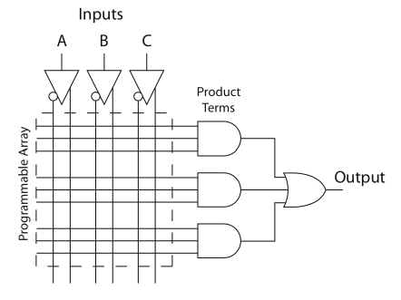
The logic algorithm is defined by choosing which input lines are connected to which product terms in the programmable array. While this architecture may seem rather limiting, in a 16V8 there are 8 independent product terms for each output line, and each product term can include all 16 available input lines. These chips can typically handle all but the most extremely complex algorithms, provided there are enough input and output lines available. Remember that in a Karnaugh map, arbitrary truth tables are also broken down into the logical OR of a number of product terms.
In "registered" mode, there is a flip-flop to latch the output value, and this value is also fed back into the programmable array, just as an ordinary input. These flip-flops must be driven by an external clock, which is typically input on pin 1.
CUPL Example
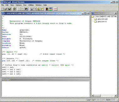
Here is simple example of a CUPL file implementing a 4-bit binary to Gray's code conversion: grayconv.pld. CUPL uses a syntax similar to C. The main parts of this file are as follows.
/*
 *
 *	University of Oregon PHYS432
 *	This program converts a 4-bit binary word to Gray's code.
 *
 */
It is always good to have some sort of descriptive header so that you can figure out what a file does when you come back to it. CUPL uses C-like comments, such that anything in between the /* ... */ pair is ignored.
Name            grayconv;
Partno          PHYS432;
Revision        01;
Date            20/03/2006;
Designer        E. Torrence;
Company         University of Oregon;
Location        None;
Assembly        None;
Device          g16v8;
CUPL files must have a header section with these nine parameters defined. Of these nine, only the name must have a real value. As this will be used to name the output JEDEC file, it must be a valid DOS filename. It is also usually a good idea to encode the target hardware device into the CUPL file in the Device field. This device identifier lets CUPL auto-select which mode to program the chip which is usually what you want.
/** Inputs **/
pin  [2..5] = [in0..3];		/* 4-bit input lines */
This defines the input lines. Pins 2-5 are given the logical names in0, in1, and so on. The [2..5] syntax is a shorthand to avoid having to explicity write out all four definitions by hand. You could also specify explicit sets as [2,3,4,5]. The actual name given to these pins is arbitrary, and in fact this statement alone doesn't specify whether these are inputs or outputs. In general, however, the logical names for a group of pins should always start at zero. Note that CUPL commands must end with a semicolon, just like C.
/** Outputs **/
pin [19..16] = [out0..3];   /* 4-bit output lines */
Here we define four output pins. Again, the name is arbitrary and just as well could have been "bob". In the Data sheet you can see that for the 16V8, only pins 12-19 can be configured as outputs. Here I have chosen the MSB to be on pin 16, to mirror the input MSB on pin 5. I could have started the inputs in this case on pin 1, although for registered PALs, pin 1 is reserved for the input clock.
/* Define Gray's code conversion as out(i) = in(i+1) XOR in(i) */
out3 = in3;
out2 = in3 $ in2;
out1 = in2 $ in1;
out0 = in1 $ in0;
This defines the actual algorithm, and also defines which pins are inputs or outputs. Different algorithms can be encoded by simply changing the logic here. The basic logical operators in CUPL are shown in the table below. CUPL can also do arithmetic operations on bit fields including multiplication and division, but the small PAL devices we are using here will quickly run out of gates to implement an algorithm like this.
| Operator | Example | Description |
| ! | !A | NOT |
| & | A&B | AND |
| # | A#B | OR |
| $ | A$B | XOR |
A very readable introduction to CUPL syntax can be found in the CUPL Tutorial. More information can be found in the WinCUPL User's Manual.
Software Resources
The CUPL compiler for Windows, WinCUPL, is freely available from Microchip who bought out ATMEL in 2016. This program is installed on the computers in Room 11, and I would encourage you to just use it there, as you also need a chip programmer for this to be at all useful. Unfortunately, I do not know of any Linux or Mac versions of CUPL, but I did once get WinCUPL working under Wine on a Mac. Since almost none of the chip programmers work on anything but Windows, this isn't really a huge limitation. If you do install WinCUPL yourself, you will need to enter a license number. This is given directly on the WinCUPL web page and is 60008009. You can enter any organization name you want.
To download the JEDEC files to the chip, we have two different programmers.
The first is an old Speedmaster LV48 programmer from IceTech. This is no longer supported by the company, but the WinLV installer still works on older PCs. This programmer needs a parallel port interface, so this may be of limited use to anyone else. At the moment, the power supply for this programmer is dead, but I will try to fix that.
We also have a slightly more modern USB-based programmer, the TL866II Plus. The software to drive this device can be found on the TL866II page.
The GQ-4x4 programmer will not program PLDs, but it will program EEPROMs. The software to drive this device can be found here. Note you must install the USB driver first (GQ USB Driver 3.0) then install the programmer (GQUSBprg 7.23).
If you are doing any real work with PLDs, you should also get to know how to use the simulator. In addition to the grayconv.pld file, one can also download the grayconv.si simulation file. This file specifies a series of "test vectors" which give the expected output for any given set of inputs. The simulation will both verify that your algorithm code is working as expected, but will also encode these test vectors into the JEDEC file. The programmer can then run the same tests on the final chip to verify that you are getting exactly what you expect.
Software Walkthrough
This is intended to give the very briefest of instructions for how to actually use WinCUPL and WinLV to program a PLD.
Step 1: Download the grayconv.pld file (and optionally the grayconv.si file) to a directory. Start the WinCUPL application, and open the grayconv.pld file. You should have a screen which looks something like this.
The main window shows the source code, while the window on the right shows files in the current project and the window on the bottom is the message window.
Step 2: Set up the WinCUPL options. Select the Options:Compiler menu, and click on the Output Files tab. Make sure the JEDEC box is checked. You can also select other output files to get a better idea what CUPL is really doing, like Fuse plot and Equations. Select the General tab and unselect Simulate. It is better to run the simulation separately, and this avoids an incorrect simulation from being written into your JEDEC file. Finally, under Options:Device click the Device in File box so that WinCUPL will auto-select the chip from the Device: field. Note that WinCUPL only recognizes Atmel chips (e.g. Atmel ATF16V8B) although the same JEDEC file will also work for the Lattice GAL16V8A/B chips as well.
Step 3: Compile the PLD file. Select the menu item Run:Device Dependent Compile (or simply click the button in the toolbar). If all goes well, there will be no compilation errors, and in the project window there will now be a grayconv.jed file (the JEDEC file, or fuse map) as well as a grayconv.doc file which is a general report listing the product terms and other useful information. You can double click on these files to see their contents. If the compliation did not succeed, try scrolling back through the message window to find the source of the error.
Step 4: Run the simulator (optional). If you also downloaded the grayconv.si file, it should also be present in the project window. Double click on this file, or launch WinSim (from Utilities:WinSim or the button on the menu bar) and open it directly. This file defines the input and output lines, plus a set of "test vectors" predicting the output for a given set of inputs. Run the simulation with Simulator:Run or the lightning bolt button on the menu bar. The simulation should be successful, and will give you a visual display of the input (in green) and the output (in blue).
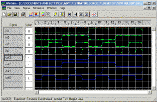
You can left click on the waveforms to change either the inputs or output values. You can also let the outputs be undetermined, and the simulator will fill them in for you. To properly check a program, however, you should have a simulation file which contains both the input and the expected output for every state. WinCUPL will compile these test vectors directly into the JEDEC file, if you have the Simulate option set under Options:Compiler, and the programmer will try this out directly on the chip.
Step 5: Programming with the TL866II. For instructions on programming with the LV48, see below. Open the Xgpro application and select the box in the upper left that says 'Select IC'. Pick the exact IC you are using from the list. Note we have both Lattice and Atmel PALs. This same process also works for programming EEProms. Click on the 'Device Info' tab at the bottom of the data window to see how to insert the chip into the socket. Place the chip in and close the clamp. Now open the grayconv.jed file produced by WinCUPL and switch back to the 'Flash' tab to see the data to be downloaded to the chip. This should have some random patterns of zeros and ones, but not all of one or the other.
Now you are ready to burn the chip. Click on the big red P icon at the top of the page to bring up the programming interface. The CODE Memory item should be selected, but the LOCK Bit should not be selected. The program shows you the chip again, so check that you have the chip inserted correctly. Select program and see what happens. I have been getting some verify errors, but the program still seems to work. If you get an overvoltage warning, try turning down the VPP programming voltage.
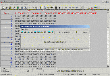
Step 5: Programming with the LV48. For instructions on programming with the TL866II, see above. Insert the PLA chip into the white LV48 programmer socket and flip the lever down to hold the chip firmly in place. The chip should have the notch facing up, but should be bottom-justified in the socket (no extra slots open below the chip). Open the WinLV program and open the grayconv.jed file produced by WinCUPL. If the (exact) correct chip is not listed on the status line on the bottom of the window, you will have to set it now. Select the menu item Programmer:Select Device. Select the plus next to either ATMEL or Lattice in the list on the left, then select PALS. This will bring up a part list on the right, and select whatever specific chip you are using. If there is a plus, select this and choose the form factor (DIP) as well. Click the accept button. You will now likely have to reload the grayconv.jed file.
You are now ready to burn the chip. Select the menu item Programmer:Operations. This will bring up a sort of dialog box with various buttons. The one just to the right of the vertical divider (Erase, Program, Verify) is what you want. If you don't get "Device Programmed and Verified" then something is wrong. If you have been playing with the simulation file, and have one which doesn't work, it is possible that the programmer has tried to verify this (incorrect) simulation against the chip and found it doesn't match. Either fix the .si file, or delete it, make a new .jed file, and try again.
A Final Note: Please don't program PLA chips over and over again just for the fun of it. There is a finite number of times these can be reprogrammed before they start to have significant failure rates. The manufacturer spec on this is 200 times, although in reality they can usually last much longer than this. If the chips in the lab are being programmed 100 times per day, however, we may not have many working chips left by the end of the year.