
Digital Electronics
PHYS 432 - FPGA Information
http://physics.uoregon.edu/~torrence/432/fpgainfo.htmlUpdated Wednesday May 05, 2021
Introduction
While it is easier to understand the concepts of combinatoric logic using discrete logic gates, any modern electronics design will some form of programmable logic instead. Field Programmable Gate Array devices (FPGAs) form a "blank slate" upon which any arbitrary combinatoric and synchronous logic can be programmed. FPGAs are an evolution of the more rudimentary PLD devices. FPGAs are also programmable logic, but they are designed to have a more flexible logic fabric, provide registers and clocks throughout to allow synchronous logic, and generally have orders of magnitude more resource available. Modern FPGAs can implement sophisticated processors within the FPGA itself (a so-called soft-core) and also can have thousands of digital logic operations occurring concurrently. Current state-of-the-art FPGAs can have millions of logic cells available. FPGAs have become widely used in applications where fast, highly parallel operations are needed, such as triggering in HEP experiments.
There are a wide variety of methods for implementing algorithms in FPGAs, generally referred to as Hardware Description Languages (HDLs). The two most common are Verilog and VHDL. These are somewhat similar to CUPL in the PLD case, and we will use Verilog because the syntax is somewhat simpler to read, making it easier for beginners to understand. There are other higher-level synthesis tools available that try to make designing complex systems on FPGAs easier. One graphical language that works with our boards is icestudio. There are even now utilities to translate python code into the equivalent digital logic.
Similar to PLDs, the verilog description file is compiled or 'synthesized' into a gate-level description that is then downloaded to the chip to implement the logic. We will use FPGAs that can be programmed over a USB interface, which is highly convenient. The programming software, or toolchain, is also available on PCs or OS X (or Linux) which makes it very flexible.
Hardware Overview
We will use an FPGA device from TinyFPGA that is provided in a DIP package for easy use in a breadboard and is programmable over a simple USB connection. The specific device we will use is the TinyFPGA BX, based on the Lattice ICE40LP8K FPGA. This has a relatively modest 7680 individual logic cells, but that is more than enough to get an idea of what an FPGA can do. The BX is a 3.3 V device, so be very careful when wiring up external logic. The BX board will accept up to +5V, and will regulate it down to 3.3V for the FPGA, but the input and output pins of the device expect 3.3V. The 3.3V outputs will work with TTL logic inputs, but the reverse direction needs a level converter. Also, applying +5V to the FPGA inputs can damage the chip, so please be careful!
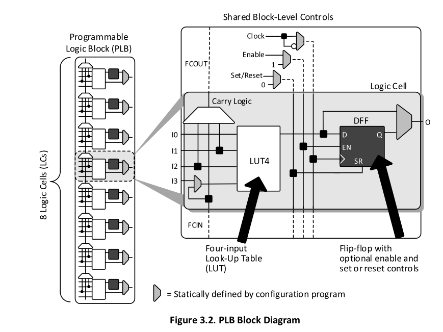
The basic FPGA architecture involves 4-bit logic cells with look-up-tables (LUTs) to implement arbitrary boolean functions and D-type flip flops to provide synchronous outputs. Eight of these logic cells are combined into a single programmable logic block (PLB) as shown below. These PLBs already allow fairly sophisticated 8-bit operations to be defined efficiently, particularly addition. The ICE40LP8K FPGA has nearly 1000 of these PLBs that can be arbitrarily connected together to create more sophisticated logic.
FPGA design follows a very similar flow as designing a circuit with discrete logic. First you should have a block-level design of the main components you want to use, and the input/output connections between those blocks are defined. Rather than discrete chips, however, the blocks are defined as modules and the connections between them are all defined in the Verilog file.
Verilog Example
Here is simple example of a Verilog file implementing a debounced button driving an 8-bit counter that is then decoded to drive 8 LEDs: buttontest.v. Verilog uses a syntax similar to C, but it is always worth remembering that this is not a procedural language, and no program is running on the FPGA. The main parts of this file are described as follows. A slightly more extensive description of verilog syntax can be found at the Verilog Wikipedia page.
// buttontest.v
//
// Debounce a button to drive an 8-bit counter.
// Use a decoder to drive a custom pattern on 8 output LEDs.
//
// look in pins.pcf for all the pin names on the TinyFPGA BX board
// Pins 2 and 13 have internall pull-up resistors enabled
//
// Synthesize and download with:
// apio build
// tinyprog -p hardware.bin
//
// E.Torrence
// PHYS 432
// April 14, 2019
//
It is always good to have some sort of descriptive header so that you can figure out what a file does when you come back to it. Verilog uses C++ style comments, so that anything on a line following the double slash is ignored. These comments are not required, however.
module top (
    input CLK,    // 16MHz clock
    input PIN_2,  // Button input
    input PIN_13, // Button input
    output LED,   // User/boot LED next to power LED
    output USBPU, // USB pull-up resistor
    output PIN_14, // 8 LED outputs
    output PIN_15,
    output PIN_16,
    output PIN_17,
    output PIN_18,
    output PIN_19,
    output PIN_20,
    output PIN_21
);
Logic blocks can be split up between Verilog files in a common directory, but one file must implement the top module. In the parenthesis after a module name, all inputs and outputs of that module must be defined. For the top module, these are usually the IO pins of the chip and the system clock. The pins.pcf pin constraint file provided for the TinyFPGA BX board defines the mapping between the FPGA pins and the numbered pins on the BX board. In addition to CLK, which gives access to the 16 MHz system clock, there are two other special pins used in this file. LED provides access to the built-in LED on the BX board, while USBPU is the USB pull-up resistor. When this is set low, it appears to the computer as though the board is not connected to the USB bus.
    // drive USB pull-up resistor to '0' to disable USB
    assign USBPU = 0;

    // This is our reset button, doesn't need to be debounced
    wire reset;
    assign reset = !PIN_13;
Outside of always blocks, a signal source is routed to an output with the assign function. Here we assign the USB pull-up resistor to be 0 (logic level LO) and we declare a new wire that will have the logical inverse of the PIN_13 logic value. Pin 13 of the BX board should have a button connected to ground. With the built-in pullup resistor enabled on Pin 13, this button provides a logic level of HI when open and LO when closed (button is pressed). The pullups must be configured in the pins.pcf file. Note the C-like syntax with a semi-colon terminating each line.
	// Output LED display, 8 bits with MSB first
    reg [7:0] LEDreg;

    // Continuously assign the value of ledreg to output pins 14-21
    assign {PIN_14, PIN_15, PIN_16, PIN_17, PIN_18, PIN_19, PIN_20, PIN_21} = LEDreg;

    // Internal counter value
    reg [7:0] countValue;
A reg is a single bit that can store a value (in contrast, a wire just carries information from one place to another). The reg [7:0] LEDreg syntax creates an 8-bit register called LEDreg. The [7:0] order specifies the bit order from MSB to LSB within the array. This can be important when applying arithmetic operations like addition, or interpreting register values as binary numbers. The following line assigns the output pin values to this array, so that if the values in LEDreg change, the output pins voltages will also change. A second 8-bit register is also created to store the current value of the 8-bit counter.
	// Instantiate a button debouncer module, output goes to button1
    wire button1;
    debounce b1(CLK, PIN_2, button1);

    // Instantiate a counter based on debounced button1 as a clock
    counter8 count8(button1, reset, countValue);
Here two logic blocks are created (they are defined further down in the file) and signals are wired as inputs and outputs to these logic blocks. In the first case, a debounce block called b1 is created, and the system clock CLK plus PIN_2 are passed as inputs, while the wire button1 is used to receive the output. This button1 wire is also connected as the input to the 8-bit counter defined by the counter8 block. Note we could have created multiple counters or other logic blocks, but each needs a unique name and must drive unique outputs. Just like in normal TTL hardware, multiple logic blocks can have the same input signals, but must have unique outputs (which could be later combined with more combinatoric logic).
    // Use counter value as input to display decoder
    displaydecoder lut(state, LEDreg);

    // Alternately, display counter value directly on LEDs
    // assign LEDreg = countValue;
A third logic block is created that takes the current counter state and acts as a decoder to create a specific pattern for the output LEDs based on the current counter state. The commented out assign statement would just wire the counter value directly to the LED output pins. If this line is uncommented, the displaydecoder line would need to be commented out, as otherwise two separate data sources would be trying to assert values to LEDreg.
All logic blocks must be defined either in this file or other Verilog files in the same directory. The logic block declaration is similar to the top module with all inputs and outputs specified. The displaydecoder module implements a look-up table that is addressed by the input argument as shown:
	// Display decoder/Look-up table
	module displaydecoder (
       input [7:0] state,
       output [7:0] display
	);

    // LUT is 8 bits wide, 16 entries (4 bits) long
    reg [7:0] lut [0:15];
    initial begin
        lut[0] <= 8'h00;
        lut[1] <= 8'h01;
        ...
    end

    assign display = ~lut[state[3:0]];

endmodule
The lut declaration is an array of 8-bit registers with 16 entries. To make use of all 8 bits of addressing would require 256 entries. The initial statement declares conditions that will happen only once when the chip is powered on. In this case, non-blocking assignments are made for all of the lut entries. The non-blocking operations (<=) indicates that these all happen in parallel, and you can not count on any execution order. A blocking assignment (=) would enforce an order of operation between the various assignments which might be needed if the outcome of one assignment is used as the input to a following assignment. Literal values are used in the assignments, with 8'h00 indicating that the number is an 8-bit hex value with value 00. The other common literal syntax is 4'b0101 which in this case indicates a 4-bit binary value with decimal value 5. Note the decimal meaning would vary depending upon which end of the register was defined as the most-significant bit. An unqualified number (i.e. without the 4'b prefix) will be interpreted as base-10 decimal. For assigning bit patterns, this is generally viewed as bad practice and error prone, although it technically works.
All outputs declared in a logic block must have values assigned to them. Here we use the value of the look-up table indexed by the lowest four bits of the input state register. The square bracket notation state[3:0] selects a 4-bit chunk of the 8-bit register (similar to python syntax). A bit-wise inversion is applied with the unary tilde operator as part of the assignment.
The final important Verilog concept can be seen in the simple 8-bit counter logic block declaration:
// Simple 8-bit counter with synchronous reset and overflow
module counter8 (
    input clock,
    input reset,
    output [7:0] count,
    output overflow
);

    // Be clear these are registers
    reg [7:0] count;
    reg overflow;

    always @ (posedge clock or posedge reset) begin
        if (reset)
            count <= 8'h00; // Set to zero

        else begin
            count <= count + 1;
            // Overflow is set when counter is resetting to zero
            overflow <= (count == 8'hFF);
        end
    end

endmodule
The always line declares a block that will always be executed (in contrast to the initial block seen before that is only executed once at startup). This always block is conditionally executed at the positive edge (rising edge) of either the clock input or the reset input. You can also define execution on change of value with syntax such as always @ (reset) begin. Within the always block, C-like conditional statements are used to decide what happens. If the reset line is HI, the counter value will be set to zero, and otherwise the counter value is decremented and the overflow bit is set. Non-blocking assignments are used throughout, which means the values don't change until all operations in the always block are completed. This means code like the following can be used to swap the values of two registers each clock cycle:
	always @ (posedge clock) begin
	    reg1 <= reg2;
	    reg2 <= reg1;
	end
The ability to mix C-like syntax for conditional statements and simple arithmetic operations (including multiplication and division) makes Verilog much more readable than purely Boolean logic languages like CUPL. One has to always remember, however, that this is not a program in the sense of a processor executing instructions. If you declare 20 versions of one logic block, all 20 will operate concurrently in parallel. Sequencing of operations must be enforced by input/output data paths and (within reason) blocking assignments in specific logic blocks.
A complete list of Verilog operations can be found on the Verilog Wikipedia page but a set of the most common operations are shown in the table below.
| Operator | Example | Description |
| Bitwise operations | ||
| ~ | ~A | NOT (bitwise inversion) |
| & | A & B | bitwise AND |
| | | A | B | bitwise OR |
| Logical operations | ||
| ! | !A | NOT (logical inversion) |
| && | A && B | AND |
| || | A || B | OR |
| Relational operations | ||
| > | A > B | Greater than |
| >= | A >= B | Greater than or equal |
| == | A == B | Logical equality |
| != | A != B | Logical inequality |
In addition to the Verilog Wikipedia page a concise primer on Verilog syntax can be found in the quick reference guide I found on the Stanford EE183 website. There are also numerous Verilog tutorials on the web if you want to dig deeper.
Software Resources
Usually, programming FPGAs involves expensive professional development environments tied to a specific vendor. As smaller FPGAs are becoming more popular, freely available development tools are starting to appear. One of the great features of the TinyFPGA BX board is the ability to program the Lattice FPGA with no additional hardware other than a USB cable. The bootloader for the FPGA is built into the fabric of the FPGA itself, with no additional chips on the board providing USB support.
In general, the three tools needed for FPGA development are a synthesis tool, a simulation tool, and a programmer. Professional FPGA design is much more about testing the logic in simulation than testing it on final hardware. Many logic issues in FPGAs can be found using logic simulations, and for professional developers this is seen as the key step in the development process. We will not discuss simulation here as our code will be quite basic, but it is worth remembering that Verilog code should pass simulation checks before it is ever downloaded to an FPGA.
TinyFPGA recommends apio as an Integrated Development Environment (IDE) to perform synthesis and simulation tasks using the lower-level IceStorm tools that have been written for the Lattice ICE FPGA family. This is a command-line tool that can also be used in graphical development environments such as ATOM. The apio commands seem to work fine on all major operating systems, so you should be able to do this on your own laptop if you really want to. For programming the boards, TinyFPGA provides the python-based tinyprog to program the boards over USB. Because the bootloading process on the TinyFPGA boards is a custom solution, this is the only option, but being python-based, it works just fine on all major operating systems.
Software Walkthrough
This is intended to give the very briefest of instructions for using the development tools to program a TinyFPGA BX on our lab computers. An installation guide is provided further below.
Step 1: Download the seconds.v Verilog file along with the pins.pcf pin constraint file. You will need both of these and the apio.ini file in a folder with no other Verilog files.
Step 2: Open a command-line application on your system and navigate to the folder containing the Verilog code. Synthesize the bytestream file with the command:
apio build
This may print some warnings about unallocated pins, but will end with Success if everything worked. You can issue the command again to be sure. The outputs of this command are bytestream files including hardware.bin that we will program to the board.
Step 3: Download the bytestream file to the FPGA. First, make sure the TinyFPGA BX board is connected with a USB cable and in bootloader mode by pressing the black button on the board. When the board is ready to be programmed, one of the LEDs should be slowly fading in and out. The board can get all of its power over USB, so the board doesn't even need to be plugged into a breadboard to be programmed or tested. Check that you can see the board over USB with this command:
tinyprog -l
If everything goes well, you should get back something like this:
    TinyProg CLI
    ------------
    Using device id 1d50:6130
    Only one board with active bootloader, using it.
    Boards with active bootloaders:

        USB 20.6: TinyFPGA BX 1.0.0
            UUID: e1ef8809-618f-4394-99ef-9fdd16ef5e4e
            FPGA: ice40lp8k-cm81
If this doesn't work, and the light is clearly fading in and out, just try again. It sometimes takes me a few times to establish communication with the board. Once tinyprog can see the board, you can download your bytestream file with this command:
tinyprog -p hardware.bin
Again, if this fails, try again. When this works, you should see obvious evidence of something being transferred and a final output that looks something like this:
    TinyProg CLI
    ------------
    Using device id 1d50:6130
    Only one board with active bootloader, using it.
    Programming USB 20.6 with hardware.bin
    Programming at addr 028000
    Waking up SPI flash
    135100 bytes to program
    Erasing: 100%|----------------------------------------| 135k/135k [00:00<00:00, 168kB/s]
    Writing: 100%|----------------------------------------| 135k/135k [00:00<00:00, 186kB/s]
    Reading: 100%|----------------------------------------| 135k/135k [00:00<00:00, 391kB/s]
    Success!
The board will immediately be put into run mode, and the downloaded logic will start executing. With the seconds.v file, the built-in LED should flash on/off with a one second period. To return to bootloader mode to program the board again, just press the black button. It can sometimes be very painful to debug an FPGA, since if things aren't working properly, there will be no output whatsoever. Often, people use the built-in LED as a status indicator and try to debug their logic that way. Hooking up external LEDs can also be useful.
Documentation
- TinyFPGA Home Page
- TinyFPGA BX Guide
- TinyFPGA git repository, includes hardware schematics and example Verilog
- Lattice iCE40 Page
- iCE40 family data sheet
- apio git repository
- apio documentation
Installation Guide
These instructions are following the TinyFPGA description here.
Step 1: Install python. Use the Windows Python Installer or the OS X Python Installer to get Python3 if you don't have it installed already. You can check your python version at the command line with python -V.
Step 2: Install APIO and tinyprog. These are the Verilog synthesis tool and the download tool respectively. Open a command line (Terminal on OS X) and install apio and tinyprog with the command:
pip install apio tinyprogOn OS X you may need to use pip3 to get the python3 version of the pip installer. If this succeeds, you can install the rest of the toolchain with:
apio install system scons icestorm iverilog
apio drivers --serial-enable
Depending on the system you may also need to first install the drivers package. If this worked, you should now be able to see the TinyFPGA BX over a USB connection. Plug the board in with a USB cable (it will draw power from the USB connection) and try the Software Walkthrough above.
Step 3:Install ATOM (optional). ATOM is an integrated development environment (IDE) recommended by the TinyFPGA website. It gives you an editor and nice interface to synthesize and program the TinyFPGA BX board. For a variety of technical reasons, I could not get this to work on either OS X or Windows. You can do everything you need directly at the command-line with apio and tinyprog. If you want to try ATOM, follow the instructions here.
Step 4:Test! You should now be able to program the FPGA. Either use the code example given above, or download the TinyFPGA BX Repository from git. If you use the git repository, go to the apio_template directory to find the top.v Verilog file and the pins.pcf constraint file. From that directory, use this command:
apio buildto synthesize the bytestream file. This should create three versions of the hardware description bytestream file in binary (.bin), Ascii (.asc), and Berkeley Logic Interchange Format (.blif). We can program the FPGA with the binary version with the following command:
tinyprog -p hardware.binIf this worked, the button should now be flashing an SOS pattern. Press and hold the button on the FPGA to return to the bootloader and allow the FPGA to be programmed again.